
Power Bank PCB Copper, Power Path & Stack-Up Reference
An engineering reference for power bank PCB current paths, copper design, connector routing, switching stages, thermal concentration, voltage drop and board stack-up decisions under higher charging loads.
High charging power has to travel through a real copper path.
Trace width, copper weight, vias, connectors, switching components and thermal concentration all influence voltage drop and sustained performance. The PCB should be reviewed together with the battery, cable and enclosure heat path.
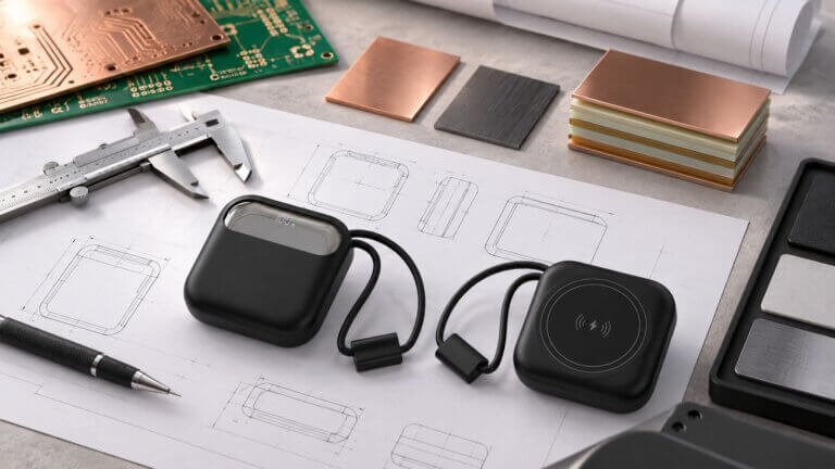
Quick Engineering Review
Review the complete high-current path instead of relying on copper thickness or component count alone.
High-Current PathReview traces, planes, vias and transitions from the cell / PACK to the output port.Power Components
Confirm MOSFETs, inductors, sensing and other critical components match the required load.Voltage Drop
Measure loss across PCB, connectors and cable transitions at the target current.Hotspots
Identify component, copper and connector hotspots under sustained load.

Buyer Decision Points
Current Path GeometryTrace width, copper planes, parallel layers and vias must support the intended current with controlled loss.Power Components
Review MOSFETs, inductors, sensing and switching components as one conversion system.Connector & Cable Transitions
Board-to-port and board-to-cable transitions can add resistance and heat.Thermal Spreading
Component placement, copper area and enclosure heat paths affect sustained target power.

Related Engineering
Thermal & DC-DC Efficiency →
Built-In Cable Loss →
Mechanical Stack-Up & DFM →
BOM & Change Control →
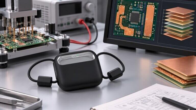
PCB & Power Path FAQ
Is PCB copper thickness enough to judge power capability?
No. Geometry, vias, power components, connectors, cable transitions and thermal spreading all matter.Does a higher component count mean a better PCB?
No. Review the actual electrical path, component ratings, measured loss and thermal behavior.Why tie test evidence to the exact PCBA revision?
Because changes in components, layout, firmware or connectors can change voltage drop, efficiency and hotspots.Additional PCB Power Path FAQ
What is a power path in a power bank PCB?
The power path is the electrical route carrying current between the cell or PACK, conversion stage, protection devices, connectors and output ports or cables.
Why do PCB trace width and via count matter?
Narrow copper or insufficient vias increase resistance, voltage drop and heat at higher current. Layout must match the intended continuous load.
How do MOSFETs affect power-bank efficiency?
MOSFET conduction and switching losses contribute to heat and voltage drop. Device selection and operating conditions affect sustained efficiency.
Why are connector transitions important in a high-current design?
Current often narrows or changes layers near connectors and cable pads. These local transitions can become hotspots even when the rest of the PCB has adequate copper.
What should be measured during power-path validation?
Measure input and output voltage, current, conversion efficiency, voltage drop and temperatures at critical components and PCB regions under defined load conditions.
How does board stack-up affect thermal performance?
Copper distribution, layer count, thermal vias and planes can spread heat and reduce local hotspots, but they must be evaluated with the actual component layout.
When should the PCB power path be revalidated?
Revalidate after changes to output power, battery configuration, major components, connector layout, copper geometry, cable interface or firmware that changes operating current.
Need to Review a High-Current PCB Power Path?
Send the target output profiles, battery configuration, board constraints and cable architecture. ZEROSET can identify the main current-path and thermal validation points for the platform.